Imagine trying to be a world-class safe-cracker. You could read every manual on social engineering to trick guards, and you could learn how to bypass the security cameras. But when you are finally standing in front of the heavy steel door, if you don’t understand how the tumblers interact, how the locking mechanism engages, or exactly where the physical vulnerabilities are in that specific metal alloy, you aren’t going to get in.
In cybersecurity, we often get caught up in the digital equivalent of dodging cameras: analyzing phishing emails, learning malware signatures, and running vulnerability scanners. We focus intensely on the software layers (the “crowd”) and the network traffic (the “paths”).
But here is the fresh perspective that many beginners miss: Every single piece of software, legitimate or malicious, eventually becomes electricity flowing through a specific piece of metal.
This is why mastering Computer Architecture and Hardware Basics is not optional; it is your fundamental master key. It transforms you from a superficial observer into a true digital surgeon. In an era where AI is automating attacks and “soft” vulnerabilities are increasingly patched, the deep, foundational flaws hiding at the hardware level are becoming the new, catastrophic battleground.
How The Computer Actually Thinks
When we talk about Computer Architecture and Hardware Basics, we aren’t talking about memorizing how to build a PC. We are talking about understanding the logical design and the physical implementation of a computing system.
At its core, any computer (from a smartphone to a supercomputer) follows the Von Neumann Model, a deceptively simple cycle: Fetch, Decode, Execute. The system fetches an instruction from memory, decodes what that instruction means, and then executes that action.
This “Fetch-Decode-Execute” cycle is the engine driving everything. And as a security professional, you need to know exactly how it can be corrupted.
At its core, a computer is just performing simple mathematical calculations and logical comparisons billions of times every second. To us, it might seem like intelligent decision-making, but it is just a play with two states: on (1) or off (0) using Fetch-Decode-Execute cycle.
Important Topics – Computer Architecture and Hardware Basics
* Von Neumann Architecture
This theoretical framework is named after Von Neumann. In this there is only one shared memory pathway for reading instruction and fetching data. The Stored-Program Concept is the theoretical pillar of Von Neumann architecture, positing that a computer’s program instructions should be stored in the same electronic memory as the data they operate on. As the data and instructions are on same electronic media and share the same memory path, it results in the idle time for CPU as only data or instructions could be transferred at a time (Von Neumann Bottleneck).
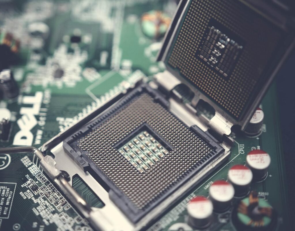
* CPU Components: ALU, Control Unit, and Program Counter
The Arithmetic Logic Unit (ALU)
The ALU is the “muscle” of the CPU, responsible for all mathematical calculations and logical comparisons. Theoretically, it handles two types of operations: arithmetic (addition, subtraction, multiplication, and division) and logic (Boolean operations like AND, OR, NOT, and XOR). When the CPU needs to make a decision—such as determining if one number is greater than another—the ALU performs the comparison and sets “flags” (status bits) that tell the rest of the processor the result. It is the only place in the architecture where actual data transformation occurs.
The Control Unit (CU)
The Control Unit is the “conductor” or manager of the processor. It does not compute data itself; instead, it directs the flow of data between the CPU, memory, and input/output devices. Its theoretical role is to decode instructions fetched from memory, translating them into a series of micro-signals that tell the ALU, registers, and other components exactly what to do. By managing the timing and synchronization of the system clock, the CU ensures that every step of a program happens in the correct order without data collisions.
The Program Counter (PC)
The Program Counter is a specialized register that serves as the CPU’s “bookmark.” In Von Neumann theory, programs are executed sequentially, meaning the CPU processes one instruction after another. The PC holds the memory address of the next instruction to be fetched. Once an instruction is successfully retrieved, the PC automatically increments its value to point to the following address. However, if a “jump” or “branch” instruction occurs (like an if statement or a loop in code), the CU updates the PC with a new, non-sequential address, allowing the CPU to skip around the program as needed.
* CPU Registers
In the orchestration of a computer’s “Fetch-Decode-Execute” cycle, CPU Registers function as the immediate, high-speed interface between the processor’s logic and the system’s memory.
General-Purpose Registers act as the primary workspace, holding the raw data and operands that the ALU requires for instantaneous calculation, thereby reducing the need for time-consuming trips to RAM.
Meanwhile, the Instruction Pointer (EIP/RIP) serves as the critical navigational tool, storing the memory address of the next command to be processed and ensuring the program flows in the correct logical sequence.
Supporting these operations is the Stack Pointer (ESP/RSP), which manages the “Last-In, First-Out” memory structure used for tracking function calls and local variables; it acts as a dynamic bookmark that allows the CPU to dive into complex subroutines and safely return to its original task.
Together, these registers form the fundamental hardware state of a running program, capturing a “snapshot” of exactly what the computer is doing at any given nanosecond.
* The Fetch-Decode-Execute Cycle
The Fetch-Decode-Execute Cycle is the fundamental operational process of a Von Neumann architecture, representing the continuous heartbeat of a computer’s processor.
During the Fetch phase, the Control Unit uses the address stored in the Program Counter to retrieve a binary instruction from system memory and move it into an internal register.
In the Decode stage, the Control Unit translates this binary pattern into specific signals, determining whether the command requires a mathematical calculation, a data move, or a logical jump.
Finally, the Execute phase carries out the instruction—often involving the ALU for arithmetic or the Stack Pointer for function management—before the Program Counter increments to point to the next instruction, beginning the cycle anew.
This repetitive loop, occurring billions of times per second in modern chips, is what allows a static set of stored instructions to transform into a dynamic, functioning piece of software.
* Virtual Memory and Paging
Virtual Memory is a sophisticated abstraction layer that allows a computer to run programs larger than its physical RAM by treating a portion of the hard drive or SSD as an extension of main memory.
Under the Paging strategy, this memory is divided into fixed-size blocks called “pages,” while physical RAM is divided into corresponding “frames.” When a program addresses memory, it uses Virtual Addresses that the hardware’s Memory Management Unit (MMU) translates into physical locations using a Page Table. If the CPU requests a page that isn’t currently in RAM, a “Page Fault” occurs, triggering the operating system to swap the required data from the disk into an available frame.
This theoretical “illusion” not only provides a massive, contiguous workspace for every running application but also ensures memory isolation, preventing one crashed program from accidentally overwriting the data of another.
* Segmentation
Segmentation is a memory management technique. In this the logical address space is divided into variable-length sections of memory called segments. This allows micro-management of memory, i.e. different permissions for different sections of program, like read-only, or execute only, etc.
While segmentation offers a natural way to organize and protect code, it introduces the theoretical challenge of External Fragmentation. Because segments vary in size, as programs are loaded and deleted from RAM, they leave behind “holes” of free space that may be too small to accommodate new, incoming segments—even if the total amount of free memory is sufficient.
* Direct Memory Access (DMA) and Security Risks
is a specialized hardware feature that allows certain peripherals—such as network cards, graphics processors, or disk controllers—to read and write directly to system memory (RAM) without involving the CPU unlike standard I/O operation. DMA hands over a “master key” to the peripheral, allowing the data transfer while the CPU focuses on high-level processing. Once the transfer is complete, the DMA controller sends an interrupt to the CPU to signal that the data is ready.
Because DMA grants a peripheral direct, unmonitored access to the system’s RAM, it creates a massive security vulnerability known as a DMA Attack. Since the “trust” is established at the hardware level, a malicious device can bypass almost all software-based security, including the operating system’s kernel protections and login screens. Attacker can use USB device to scan entire RAM and steal data, can directly access kernel and overwrite or compromise it, etc.
* Northbridge and Southbridge (Legacy) vs. Modern SoC
In the classic Northbridge and Southbridge architecture, the motherboard’s chipset was split into two distinct hubs to manage data flow. The Northbridge acted as the high-speed gatekeeper, sitting physically closer to the CPU to manage “fast” communications with RAM and the Graphics Card (AGP or PCIe). Because these components required massive bandwidth and low latency, the Northbridge was directly connected to the CPU via the Front-Side Bus (FSB). Conversely, the Southbridge handled the “slow” peripherals, such as hard drives (SATA), USB ports, audio, and networking. It didn’t communicate with the CPU directly; instead, all its data had to pass through the Northbridge first, creating a multi-step journey that was efficient for the time but eventually became a bottleneck as component speeds increased.
The transition to the Modern System on a Chip (SoC) represents a radical consolidation where these separate controllers are integrated directly into the CPU die itself. In a modern processor, like an Apple M-series or an Intel Core Ultra, the functions of the Northbridge have been absorbed into the On-Die Memory Controller and PCIe lanes, while the Southbridge functions are now handled by an integrated Platform Controller Hub (PCH) or a localized I/O die. This “all-in-one” philosophy drastically reduces the physical distance data must travel, cutting down on latency and power consumption.
* The Bootloader Sequence
The Bootloader Sequence is the critical bridge between a computer’s powered-off state and a fully functioning operating system, functioning as a multi-stage “handoff” of control. When power is first applied, the CPU initializes and executes the Firmware (BIOS or UEFI) stored on a non-volatile chip, which performs a POST (Power-On Self-Test) to ensure hardware like RAM and the GPU are operational. Once the hardware is validated, the firmware searches for a “bootable” device and loads the Primary Bootloader—traditionally located in the Master Boot Record (MBR) or an EFI System Partition—into memory. This small piece of code has one specific job: to locate and launch a more complex Secondary Bootloader (like GRUB or the Windows Boot Manager). This final stage loads the OS Kernel into RAM, initializes the system’s drivers, and hands over total control of the hardware to the operating system, completing the transition from a “dumb” machine to a programmable environment.
* Secure Boot and Measured Boot
Secure Boot is a security standard developed for the UEFI (Unified Extensible Firmware Interface) that ensures a computer boots using only software that is trusted by the Original Equipment Manufacturer (OEM). The process works through a “chain of trust” based on digital signatures; at each stage of the boot sequence, the firmware verifies the cryptographic signature of the next component—such as the bootloader, the OS kernel, and critical drivers—against a database of authorized public keys stored in the motherboard’s non-volatile memory. If a component has been modified by malware (such as a rootkit) or is unsigned, the firmware will refuse to execute it, effectively “locking the door” before an unauthorized or compromised operating system can ever gain control of the hardware.
Measured Boot, while complementary to Secure Boot, operates on a different principle: it does not block the boot process but rather creates an unforgeable “audit log” of everything that happens during startup. Using a Trusted Platform Module (TPM), the system “measures” (hashes) each piece of code and configuration data before it is executed and stores these measurements in the TPM’s Platform Configuration Registers (PCRs). Because these values are stored in a hardware-isolated chip, they cannot be altered by the CPU or the operating system later. This allows for Remote Attestation, where a corporate network or a security service can inspect these measurements to verify that the computer is in a known-good state—ensuring that even if the machine booted, it hasn’t been subtly tampered with in ways that Secure Boot might have missed.
* Root of Trust
The Root of Trust (RoT) is the foundational source in a computing system that is inherently trusted to be secure, serving as the starting point for all subsequent security operations. Because it sits at the very bottom of the computational stack—often embedded in immutable hardware or read-only firmware—it cannot verify itself; instead, it provides the “bedrock” from which a Chain of Trust is built. In a typical boot sequence, the RoT performs the first cryptographic check on the initial piece of code, which then checks the next, and so on. If the Root of Trust is compromised, the security of the entire system collapses, as there is no longer a reliable mechanism to distinguish between authorized software and malicious interference.
* Trusted Platform Module (TPM)
The Trusted Platform Module (TPM) is a specialized, dedicated microcontroller designed to provide hardware-based security functions for a computing system. Unlike software-based security, which is vulnerable to manipulation by high-level malware or administrative overrides, the TPM is physically isolated from the main CPU, acting as a “secure vault” for sensitive cryptographic data. Its primary theoretical role is to generate, store, and protect cryptographic keys, ensuring they never leave the hardware boundary in an unencrypted state. By providing a unique, hard-wired identity for the machine, the TPM enables features like disk encryption, where the decryption key is “bound” to the specific hardware; if the hard drive is stolen and placed in a different computer, the TPM will refuse to release the key, rendering the data unreadable.
* Hardware Security Modules
Hardware Security Modules (HSMs) are high-performance, tamper-resistant physical devices designed to safeguard and manage the entire lifecycle of cryptographic keys within a secure, isolated environment. Unlike a TPM, which is a small chip tied to a single local device, an HSM is a powerful enterprise-grade appliance—often a network-attached server or a PCIe expansion card—that serves as the Root of Trust for an entire organization’s infrastructure. Its theoretical advantage lies in “hard” isolation: cryptographic operations like encryption, decryption, and digital signing occur entirely within the HSM’s secure boundary, ensuring that private keys are never exposed to the host operating system or memory where they could be “scraped” by attackers.
In 2026, HSMs are the gold standard for high-stakes environments such as banking (processing thousands of transactions per second), government communications, and cloud-based Certificate Authorities.
* Firmware Integrity and Cryptographic Signing
Firmware Integrity is the theoretical assurance that the low-level code governing a device’s hardware remains exactly as the manufacturer intended, free from unauthorized modifications or “bit rot.” In 2026, this is enforced through Cryptographic Signing, a process where a vendor generates a mathematical hash of the firmware binary and encrypts it with a private key to create a digital signature.
When the device receives an update or begins its boot sequence, it uses a corresponding public key—embedded in the hardware’s Root of Trust—to decrypt the signature and verify that the calculated hash matches the original. This mechanism ensures both authenticity (the code truly came from the vendor) and integrity (the code hasn’t been altered by a single bit); if the hashes do not align, the system recognizes a “Signature Mismatch” and halts execution to prevent a potentially catastrophic security breach or system failure.
* Intel Management Engine (ME) and AMD Platform Security Processor (PSP)
The Intel Management Engine (ME) and AMD Platform Security Processor (PSP) are isolated, secondary microprocessors embedded within their respective CPUs that operate independently of the main operating system. The Intel ME is a dedicated controller that runs its own microkernel (often Minix) and remains active as long as the motherboard has power, even if the computer is turned off. Its primary theoretical role is to facilitate system management, security, and remote administration (via Intel AMT), granting it “Ring -3” privileges—meaning it has more authority over the hardware than the OS or the user. While this allows IT departments to fix a broken computer over a network, it has faced significant criticism from privacy advocates because it operates as a “black box” with a full network stack and direct access to system memory, creating a theoretical backdoor that could be exploited by sophisticated malware or state actors.
The AMD Platform Security Processor (PSP), officially known as AMD Secure Technology, serves a similar role but with a different architectural focus. Rather than prioritizing remote management like Intel, the PSP is designed primarily as a Trusted Execution Environment (TEE) to handle high-stakes security tasks such as hardware-based encryption key management, secure boot validation, and the initialization of virtual machine security. In 2026, researchers have highlighted a key theoretical advantage: unlike the Intel ME, the AMD PSP typically lacks a built-in network stack, meaning it cannot communicate over the internet independently of the main CPU. This significantly reduces its remote attack surface, requiring an attacker to have local or physical access to exploit it. Despite these differences, both technologies remain controversial “blobs” of proprietary code that are nearly impossible for a user to fully disable or audit, making them a central point of debate in the quest for truly “trustworthy” hardware.
Learning the System, Not Just the Signature
This is the perspective shift. Proper study of Computer Architecture and Hardware Basics changes you. You stop being a passive user of security tools and become an active investigator.
Here is what you gain:
- You See the “Why,” Not Just the “What.” You won’t just know that malware is “hiding.” You will understand that it might be operating at the Ring 0 (Kernel) or even Ring -1 (Hypervisor) or Ring -3 (System Management Mode) architectural layers—places your standard antivirus simply cannot see.
- You Know Where to Hunt. When analyzing network traffic, you won’t just see ports; you’ll understand how that traffic eventually interfaces with a system’s network stack (OS software) and the underlying Network Interface Card (NIC – hardware).
- You Can Defend Future-Proof. Malware signatures change daily. But the fundamental way a CPU fetches code or memory stores bits changes every 10-15 years.
Conclusion
In 2026, the cybersecurity landscape will not be conquered by those who can merely run a script. It will be mastered by those who can decompose an attack all the way down to the metal.
Proper, thorough study of Computer Architecture and Hardware Basics is mandatory because your job isn’t to protect software—it’s to protect systems. Those systems are composed of code and silicon, logic and electricity.
If your learning stops at the software layer, you are only protecting half of the system. In this field, a data leak can be caused by a software “sql injection,” but a catastrophic breach can be caused by a physical “rowhammer” bit flip.
Your roadmap is clear. Mastering the digital code starts with understanding the machine. Master the machine, and you truly master the code.
Pingback: Roadmap to the Cybersecurity world - The Cyber Server